


What is it all about?
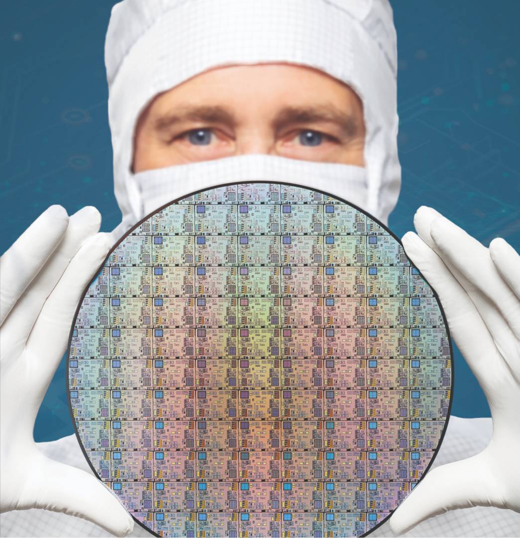
The processor in your smartphone is a prime example of advanced microelectronics. The start of its journey is a large silicon crystal that is cut into thin slices (wafers). In a semiconductor fab, billions of tiny transistors are built onto these wafers in multiple layers. These wafers are then diced into individual chips, which are attached to legs and packaged in housings. The finished processor eventually finds its place in a smartphone, laptop, refrigerator, or perhaps in the control electronics of a car.
Microelectronics includes not only the machines and processes that make this possible, but also the research needed to develop and interconnect ever-smaller and more efficient structures.
Microelectronic components are what make high-speed Internet, optical communications technology, advanced AI systems and self-driving cars possible.
Microelectronics in Berlin Brandenburg
The capital region is home to leading scientific institutions and companies in the fields of semiconductor materials for electronics and optoelectronics, chip development, special packaging technology and system integration. Microelectronics and photonics are closely interlinked in these areas.
In the capital region, established players in microelectronics meet a dynamic start-up scene, enabling innovative ideas to be promoted and implemented regionally. This network is further expanded and supported by regional and national initiatives such as the Research Fab Microelectronics Germany FMD, which has a strong presence in Berlin and Brandenburg.

»Regionally, we combine microintegration in the form of advanced packaging, which is becoming increasingly central to microelectronics, with photonics.«
– Hon. Prof. Dr. sc. techn. et Dr. Ing. Hans Richter, CEO of Gesellschaft zur Förderung von Wissenschaft und Wirtschaft - GFWW - e. V., Frankfurt (Oder)
Outlook
The rapid development of AI, autonomous driving and the call for greater sustainability require microelectronic components that deliver more performance with less energy and material consumption.
As microelectronics approaches the physical limits of pure electronic circuits in some areas, the hybrid integration of photonics and microelectronics is becoming increasingly exciting. The already close integration of photonics and microelectronics will be further promoted in the Capital Region in the future.
The capital region will make an important contribution to the current European and national efforts to strengthen technological sovereignty in the microelectronics value chain and to provide innovative solutions for future hybrid module and system integration. The strong regional expertise in photonics and the dynamic ecosystem lead to a very promising development of regional microelectronics.